Blog
Imec, ASML and TSMC develop integration route for 2D-material based nFETs and pFETs
For the first time, scaled nFETs (implementing MoS2 as the channel material) and pFETs (either WS2 or WSe2-based) with 50nm contacted poly pitch (CPP) could be demonstrated, with good current-voltage characteristics.
These results represent a crucial step in the lab-to-fab transition of 2D-material based transistors, envisioned for ultra-scaled logic as well as for back-end and wafer backside applications.
2D transition metal dichalcogenides (TMDs, such as MoS2, WS2, and WSe2) have the potential to extend and augment the logic scaling technology roadmap.
When integrated as atomically thin conduction channels replacing Si, these materials enable high-performance scaled transistors – attractive for ultra-scaled logic as well as for back-end-of-line and wafer backside applications.
They owe this promise to their good electrostatic channel control while maintaining acceptable carrier mobilities, even at ultra-scaled gate and channel lengths.
But the path to industrial adoption has so far been hampered by the lack of a 300mm integration route that can offer TMD-based n and pFETs at industry-relevant dimensions, while preserving the performance that has extensively been demonstrated on a lab scale.
ASML, TSMC and imec and now present a scalable, back-end-compatible 300mm integration approach for TMD-based n and pFETs, which has led to three key outcomes:
(1) scaled n and pFETs with 50nm contacted poly pitch (CPP) – a world first;
(2) very low off current (Ioff) at zero gate voltage (Vg=0V) for both transistor polarities;
and (3) pFETs with WSe2 channel performing close to record lab-based devices.
With 94% operational transistors (i.e., with Imax/Imin >105), the CMOS-like integration approach – with n and pFETs integrated on the same 300mm wafer – is proven to be robust and stable.
The proposed process flow is applicable to 2D channel materials other than MoS2, WS2, and WSe2.
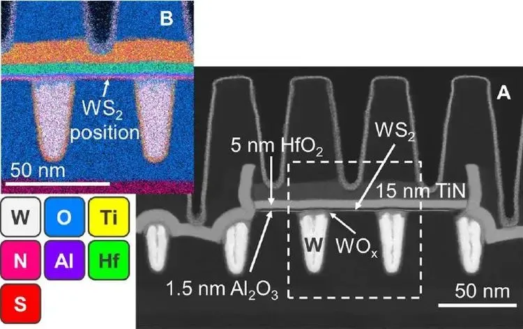
Gouri Sankar Kar, VP R&D compute and memory device technologies at imec: “Transistors based on 2D TMD materials are typically optimized for small channel lengths. However, they usually have a large contact area to keep the contact resistance as low as possible, hindering further scaling. For the first time, we achieved 50nm CPP – a metric determined by both the gate length and source/drain contact length – without affecting the performance of the 2D n and pFETs. The use of single-patterning EUV lithography, optimized in close collaboration with ASML, was key in enabling the scaled CPP.”
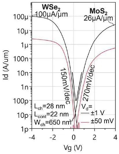
The scaled transistors show good current-voltage characteristics, with pFETs performing nearly as well as the best performing lab-based devices – addressing a long-standing challenge for TMD transistors. In addition, electrical results show that both transistor polarities turn off when the gate voltage (Vg) is set to 0V. “This ideal behavior can be ascribed to the use of an innovative ‘reverse’ thin-film transistor (TFT) fabrication flow,” explains Gouri Sankar Kar. “Unlike conventional 2D-material based transistors, our n and pFETs have bottom contacts and an overlapping deposited gate. This is realized by transferring the TMD channel material onto already pre-patterned tungsten (W)-filled trenches working as the contacts. ”
Highlighting the strategic importance of the research work, Dr. Min Cao, TSMC’s Vice President and CTO remarked, “Our research collaboration is instrumental in pushing the boundaries of semiconductor innovation. The focus is on de-risking and accelerating the ‘lab to fab’ transition, ensuring that groundbreaking discoveries – especially in these novel channel materials – could be rapidly and efficiently integrated into advanced manufacturing, and ultimately deliver cutting-edge solutions.”
“2D TMD materials could potentially enable much smaller and higher-performance transistors than those based on silicon, but 2D-channel devices that have been demonstrated so far using 300mm processes are actually fairly large, and patterned using older lithographic technologies. Thanks to the much sharper resolution of EUV lithography, we were able to create TMD transistors with channel lengths as small as 28 nm, and at a pitch compatible with the most advanced transistor nodes.” added Etienne De Poortere, Director Technology Development Center Europe of ASML.
See all our Imec content.