Blog
AMD “Zen 7” IP to Use TSMC A14 Node and More Advanced Packaging

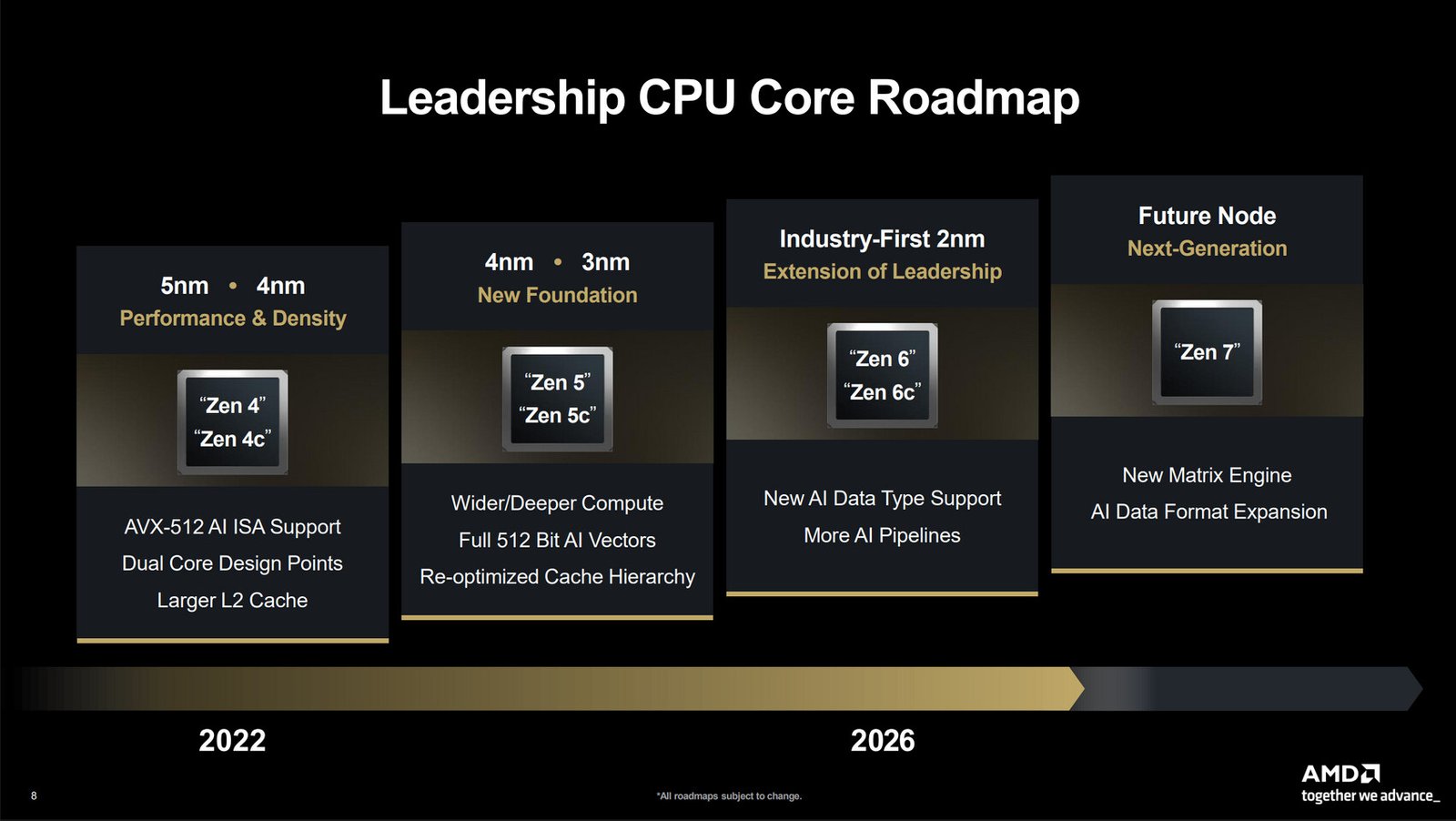
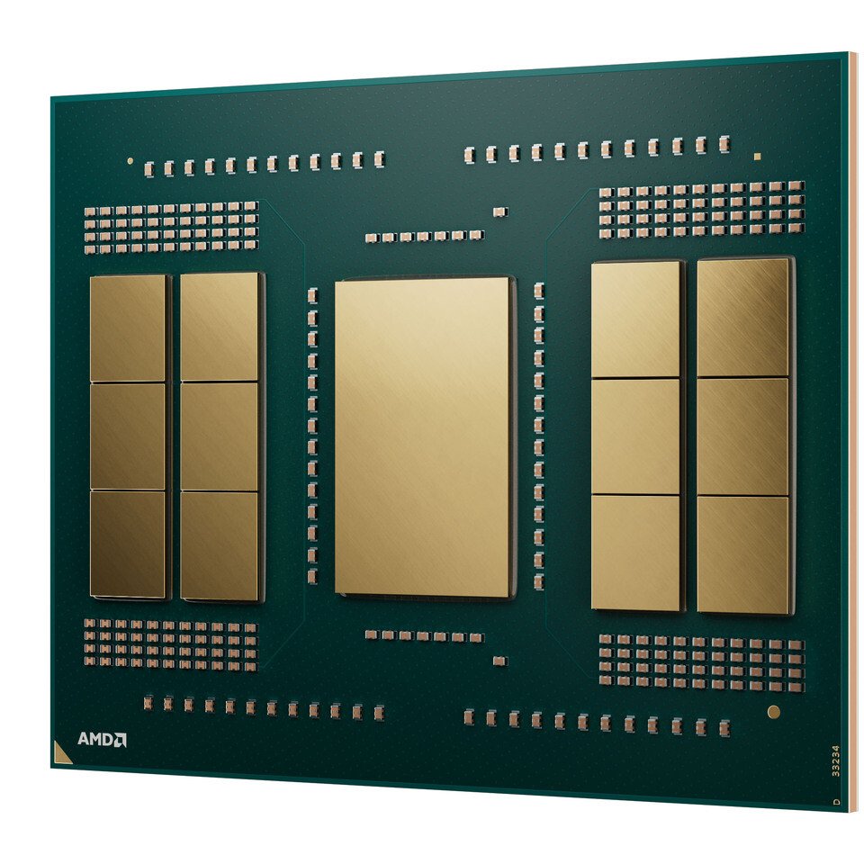
For “Zen 7” CCD IP codenamed “Grimlock,” AMD plans to make its CPU architecture more AI-relevant, allowing future processing workloads to better leverage the processing power of 16 CPU cores per CCD. Among the key features are AVX10 and ACE. AVX10 unifies AVX-512 and AVX2 features to improve performance and compatibility across vector math-heavy workloads. ACE, or Advanced Matrix Extensions for Matrix Manipulation, is an industry-standard matrix math instruction set that could be relevant to a wide range of devices, from smartphones to servers. Other ISA additions with “Zen 7” include FRED (Flexible Return and Event Delivery), which replaces the current device interrupt model to reduce system-level latency. “Zen 7” also implements ChkTag x86 Memory Tagging to counteract various memory-level data vulnerabilities caused by buffer overflows and use-after-free errors.
Finally, AMD is reportedly exploring various packaging technologies, including next-generation 3D V-Cache technology. The company is said to be evaluating Powertech’s FOPLP (Fan-Out Panel-Level Packaging) solution. Powertech, a silicon packaging vendor based in Taiwan, is recognized as one of the leading OSAT companies. As AMD explores different supply chain providers, Powertech has reportedly emerged as a potential option. The company currently offers various FOPLP technologies, so we are eager to see what AMD might choose for its “Zen 7” designs as it seeks to shift away from TSMC’s dominance in silicon packaging.