Blog
Building Nanodevices Using CMOS Processes
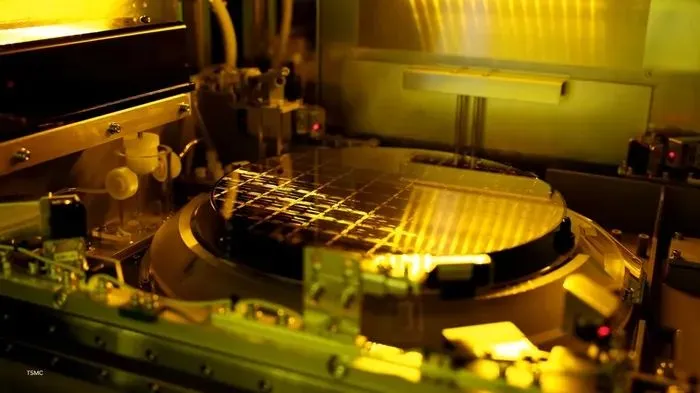
Our world has been changed by microelectromechanical-systems (MEMS) devices such as sensors — they’re smaller, more efficient, and usually more accurate than their legacy predecessors. MEMS technology is based on an extended form of traditional IC manufacturing, where complex nanoscale microstructures are built by repeating processes from film deposition to etching.
Recently, Nanusens has begun making nanoscale structures within the layers of a CMOS chip using standard processes in CMOS fabs. The resulting MEMS sensors and required control circuitry form single-chip solutions that are significantly smaller than their current, multi-component counterparts. Many different sensors can be built into the same tiny chip to enhance the user experience and differentiate products without taking up more space.
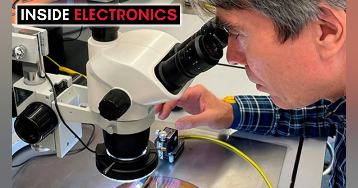
We sat down with Nanusens CEO Dr. Josep Montanyà Silvestre to talk about the industry, the company, and its technology. The company manufactures single-chip solutions with a packaged size of only 0.5 mm3. Nanusens uses 0.18-micron CMOS technology, which is a well-established, high-volume technology that makes it possible to use any fab.