Blog
TSMC and Sony Team Up on Next-Gen Image Sensor and New Production Lines for AI
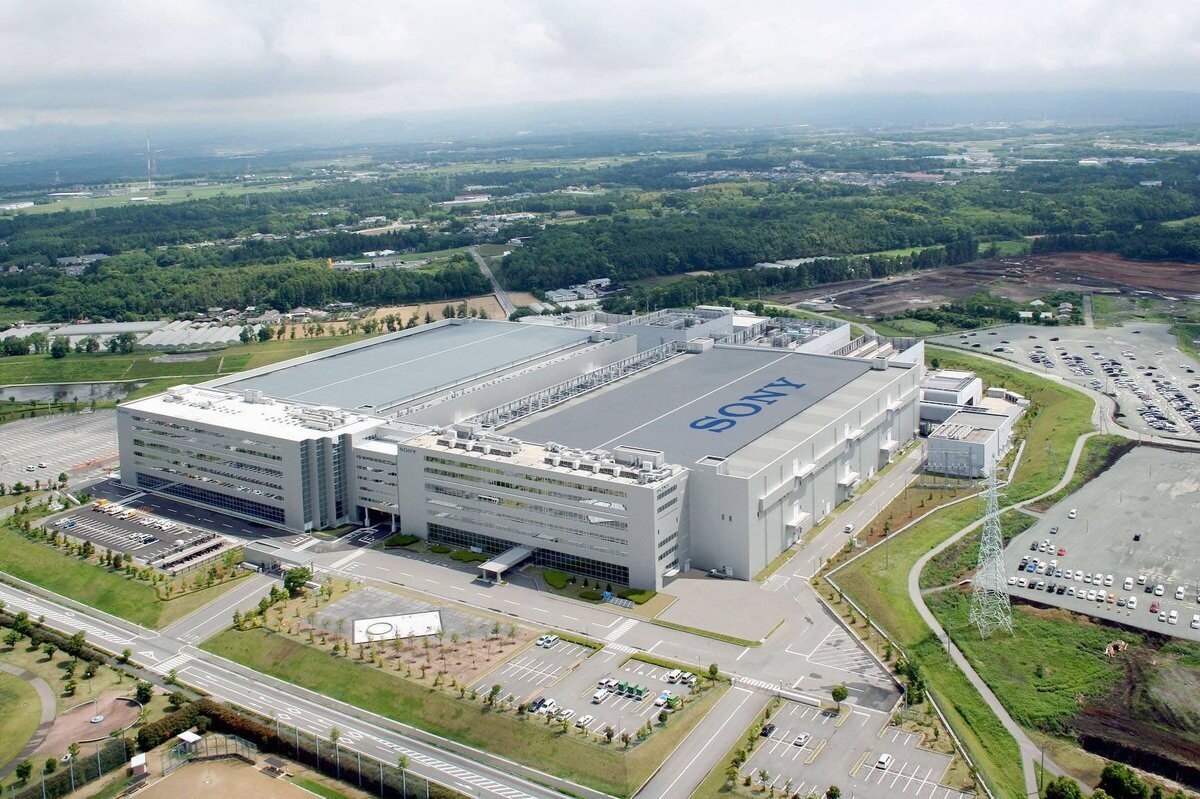
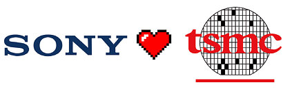
Sony Semiconductor Solutions and TSMC have signed a non-binding memorandum of understanding to form a joint venture focused on next-generation image sensor development and manufacturing. Sony will be the majority and controlling shareholder in the joint venture, which plans to set up development and production lines at Sony’s newly built fab in Koshi City, Kumamoto Prefecture. The partnership brings together Sony’s image sensor design expertise and TSMC’s process technology and manufacturing scale. Beyond conventional imaging, the two companies are also looking at opportunities in physical AI applications, automotive and robotics specifically, where high-performance sensing is becoming increasingly important. Investment plans for the joint venture are still being worked out, and Sony is also considering additional capital investment in its existing Nagasaki plant. Both are being planned in phases based on market demand and are contingent on Japanese government support. Earlier reporting from Reuters indicated Japan’s Ministry of Economy, Trade and Industry (METI) has confirmed subsidies of up to ¥60 billion (around $380 million) for Sony’s Kumamoto image sensor facility. 
The timing makes sense for both sides. TSMC is already involved in Kumamoto through its first fab there, which entered mass production in late 2024 supplying Sony Semiconductor Solutions and DENSO on 22/28 nm and 12/16 nm nodes. The new joint venture would push that relationship into more advanced territory. For Sony, the move comes as competitive pressure in the image sensor market is building as Samsung has been gaining ground in supplying sensors for Apple, squeezing Sony’s position in a segment it has long dominated. However, the joint venture still needs a definitive legally binding agreement before it’s official.
Related Posts
Sony Highlights PlayStation AI Usage in Legal Documentation
As we've seen previously, many modern game studios are leaning on artificial intelligence to accelerate game development...
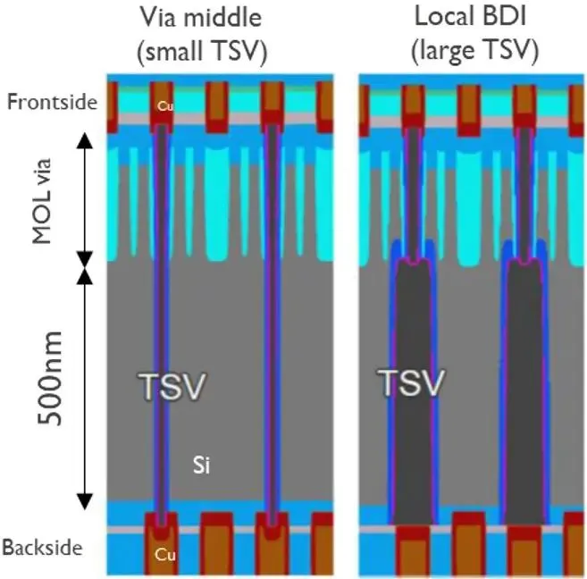
Imec and Sony develop backside interconnect integration module
The module is structured around a self-aligned local backside diel...
PhotonPath and Xiver hook up for Oxyn production
The partnership enables the transition of Oxyn manufacturing to Xiver’s 200...
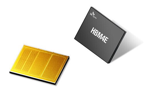
SK hynix Ships Samples of 12-Layer Next-Gen HBM4E
SK hynix Inc. announced today that it has shipped samples of HBM4E, a next-generation DRAM for AI, to major customers. "...
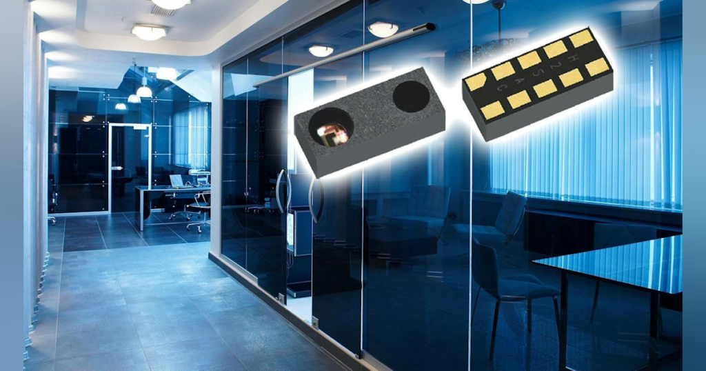
Vishay High-Sensitivity I2C Optical Proximity Sensor Detects Up to 600 mm
Proximity sensors are literally and figuratively the often-invisible elements in systems as they react to motion, positi...
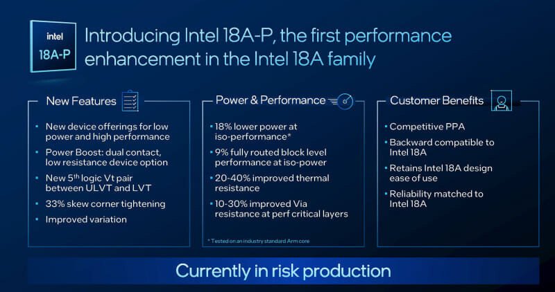
Intel Details 18A-P Foundry Node Powering Next-Gen Xeon “Diamond Rapids” Processor
At the VLSI Symposium held in Hawaii, Intel unveiled the new Intel 18A-P foundry node, a significant refinement of the I...
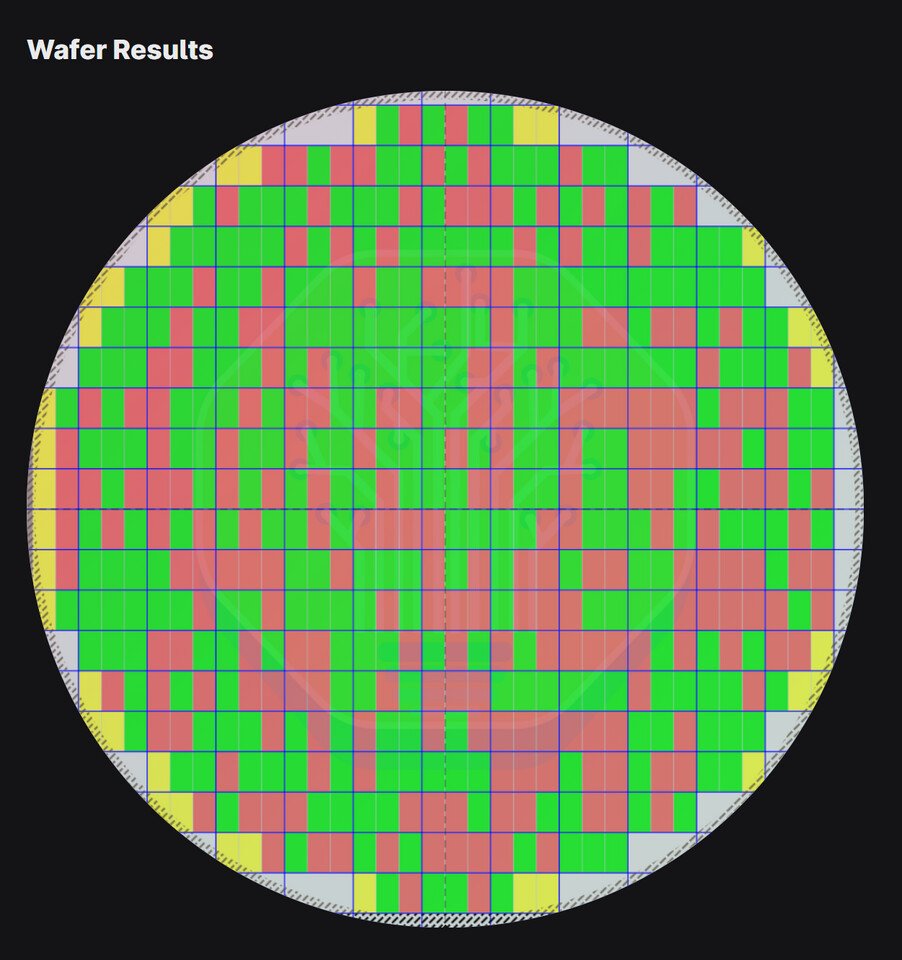
Intel 14A Yields Hit Impressive Milestone Before Trial Production
According to the latest research f...
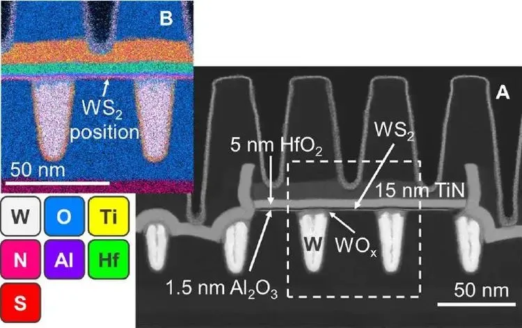
Imec, ASML and TSMC develop integration route for 2D-material based nFETs and pFETs
For the first time, scaled nFETs (implementing MoS2 as the channel material...
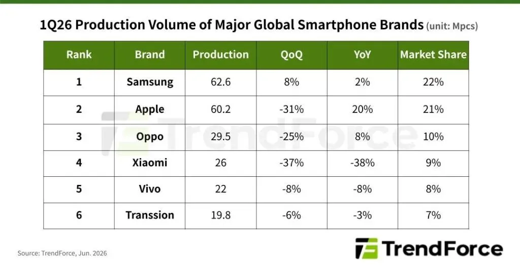
Q1 smartphone production down 1.7%
Despite a sharp rise in memory prices since the second half of 2025, the ef...
Montage Technology Samples 9200 MT/s DDR5 RCD to Boost Next-Gen Server Performance
Montage Technology today announced the sampling of its Gen 6 DDR5 Registering Clock Driver chip (RCD06) with key custome...
TSMC May revenue up 30% YoY
TSMC’s may revenue was 30% up YoY 2026 at $13.3 billion. It was an increase ...