Blog
Intel Foundry Combines GaN and Silicon Semiconductors on a Single Thin Chip
Intel manufactured the GaN wafer with silicon combined on the 30 nm process, which reportedly demonstrated excellent properties. This includes stable current carrying, very low power loss, and the ability to block voltages up to 78 V without leakage. What is fascinating is that GaN is usually used for wide bandgap applications, with high radio frequency performance exceeding 300 GHz. GaN also provides much better power delivery due to its superior material properties and operates more stably at higher temperatures. This is especially significant for workloads like electric vehicles or data center point-of-load delivery, where space is limited, temperatures can reach about 150°C, and stability is crucial.
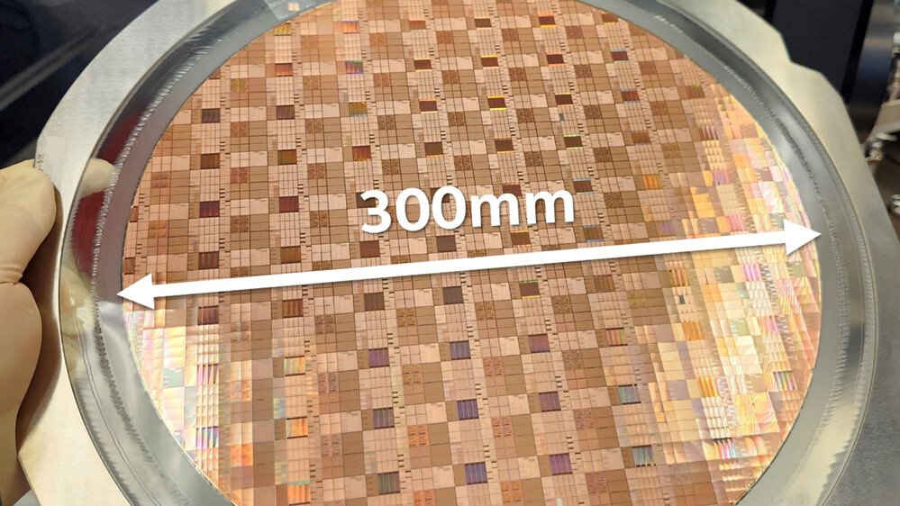
Finally, Intel used a combination of traditional logic elements like inverters, NAND gates, multiplexers, ring oscillators, and more, all of which have been tested. The electrical properties of these circuits met the latest standards, achieving switching times of just 33 picoseconds, or 33 trillionths of a second, consistently across the entire 300 mm wafer that Intel produced. The new technology is proving to be promising due to its electrical properties, yield, and performance. Intel can potentially manufacture this at scale, which means we could see many future robotics and AI data center components integrating these chips.