Blog
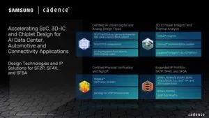
Cadence and Samsung Foundry enable 2nd gen 2nm
The collaboration delivers a signoff‑ready platform for next‑generation AI infrastructure and physical AI designs across data mcentre, edge and intelligent devices.
This broadens the Cadence IP portfolio including NVLink-C2C-enabled interconnect and CUDA-X GPU-accelerated libraries spanning high-speed SerDes, PCIe, UCIe and all leading memory interfaces on second-generation 2nm.
It enables certified Cadence flows so ecosystem partners can implement large AI, HPC and advanced system designs with higher performance, lower power and faster time to tapeout.
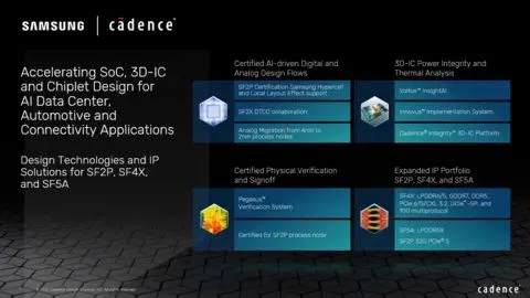
The design flow includes Cadence’s Innovus Implementation System for digital implementation, Virtuoso Studio for analogue and custom design, Integrity 3D‑IC Platform for full 3D‑IC system planning and implementation, Voltus IC Power Integrity Solution for power integrity and system‑level power analysis, and Quantus Extraction Solution and Tempus Timing Solution for signoff.
Genus Synthesis Solution’s glitch power optimisation is in the place and route flow, and a smart hierarchical flow to achieve optimal performance, power, and area (PPA) and turnaround time (TAT).
Samsung 3D Cube-H design is enabled with a full system planning, implementation and signoff flow for hybrid copper bonding (HCB) technology, including Cadence CerebrusIntelligent Chip Explorer, Integrity 3D‑IC, Innovus Implementation, Voltus IC Power Integrity (ERA) and Pegasus Verification System.
It includes silicon interposer auto-routing and optimisation, and ensures tighter connectivity between analysis, signoff, and verification, with Tempus and Pegasus.
See all our Cadence content.