Blog
Terafab’s Cost Could Reach $119 Billion as First Phase Starts at $55 Billion
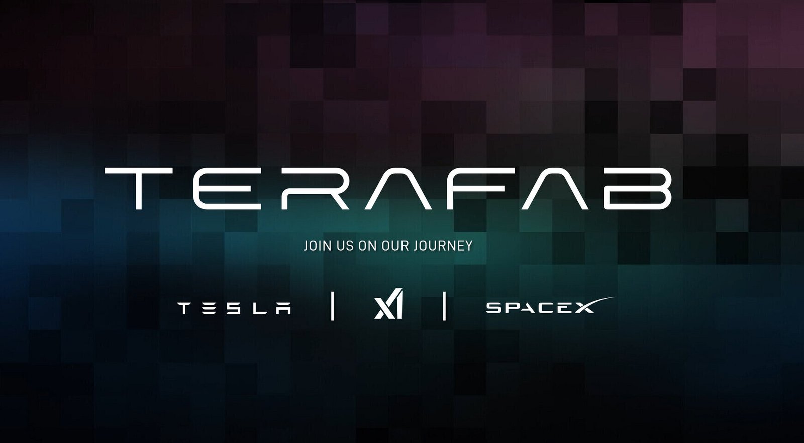
The goal of Terafab is to consolidate the entire chip manufacturing process under one roof. The plant is expected to integrate several stages of semiconductor production at a single site, including logic fabrication, memory, packaging, testing, and mask production. This setup is unusual, as these steps are typically spread across multiple specialized facilities and companies. The idea behind Terafab is that consolidating these processes could accelerate development by allowing engineers to design, test, and revise chips with fewer delays, essentially enabling rapid prototyping. This contrasts with the traditional, lengthy process of manufacturing chips at one site, packaging them at another, and testing them in-house. A typical semiconductor fab for nodes below 3 nm costs over $20 billion, but that only covers silicon manufacturing. Terafab’s goal to handle everything will push that cost astronomically high.
We know that Intel has joined forces with Terafab, and Tesla has signed on as Intel’s first major 14A customer for Elon Musk’s Terafab AI chip complex in Austin. However, the details of this deal are still unknown, and it’s unclear if Terafab will license the 14A node PDK. Additionally, throwing more funds at a problem doesn’t guarantee a solution. Building a competitive fab from scratch would require years of execution, including procuring parts from companies like ASML, Lam Research, KLA Corporation, and Tokyo Electron. For example, these companies receive orders years in advance before shipping the machinery to TSMC, Samsung, or Intel. Thus, creating a supply chain for equipment, raw materials, and other necessary components will take years to come to fruition.