Blog
Infineon expands CoolGaN BDS family

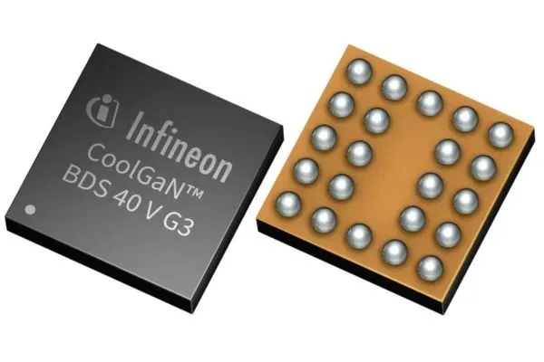
The new additions reduce PCB footprint by up to 82% and cut component count in half. For engineers designing within the strict spatial constraints of modern smartphones, notebooks and wearables, this is a significant and quantifiable step forward.
Targeting compact consumer devices the new devices give power system designers greater flexibility to optimise efficiency and streamline designs without sacrificing performance.
“As consumer devices continue to shrink while power demands grow, engineers face increasing pressure to deliver more from less. The new CoolGaN BDS devices directly address this challenge,” said Johannes Schoiswohl, GaN business line head at Infineon. “Each device integrates the function of two back-to-back silicon mosfets into a single component, reducing component count by half and simplifying PCB layouts. Design teams can leverage existing driver layout, avoiding costly redesigns and accelerating time to market. The result is a leaner and more cost-effective power path.”
The BDS, like other GaN devices, is compatible with 5V gate drive. Offered in WLCSP chip-scale packages measuring 2.1×2.1mm² and 1.7×1.2mm², the IGK048B041S and IGK120B041S are engineered for the tight spatial constraints of smartphones, notebooks and wearables.
The larger GaN device achieves 4.2mΩ RDD(on) while the smaller device delivers 9mΩ RDD(on). The CoolGaN BDS devices further distinguish themselves through superior switching and leakage performance. Gate charge is up to approximately 40% lower than comparable competing devices.
Lower gate charge translates directly to faster switching transitions, reduced switching losses and improved system efficiency in fast-charging applications.
Additionally, Drain-Drain Leakage current is more than 85% lower than competing solutions, underscoring the inherent leakage advantages of GaN technology.
Together, these characteristics reduce thermal rise, supporting long-term reliability and helping manufacturers meet increasingly stringent safety requirements.
Unlike silicon mosfets, which rely on a body diode that can allow unintended current flow, the CoolGaN BDS devices allow bidirectional voltage and current blocking.
This true bidirectional blocking capability is essential for applications such as USB overvoltage protection in smartphones and portable devices, where preventing unwanted reverse current is critical to protecting sensitive downstream components.
The devices are equally suitable for load switching and power multiplexing functions in multi-rail power architectures, where precise control of current direction across multiple supply rails is required.
With the addition of these two devices, the Infineon CoolGaN BDS 40V G3 family now comprises three devices – the IGK048B041S, IGK120B041S and the previously released IGK080B041S – addressing the full spectrum of mobile power switching requirements from compact wearables to high-performance notebooks.
Infineon had more than 40 new GaN product announcements in the last year and is on track with its implementation of scalable GaN manufacturing on 300mm wafers with first samples already being shipped to customers. 300mm GaN enables higher production capacity and faster delivery of high-quality GaN products, which further strengthens Infineon’s position in the GaN market.
The IGK048B041S and IGK120B041S are available now.
Detailed product information, datasheets and ordering options are available here.
See all our Infineon Technologies content.