Blog
Huawei looks to 1.4nm by 2031

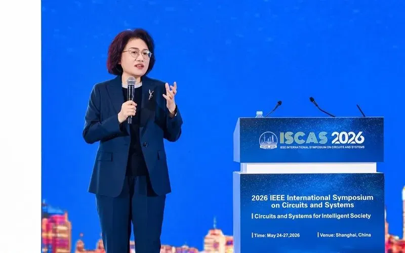
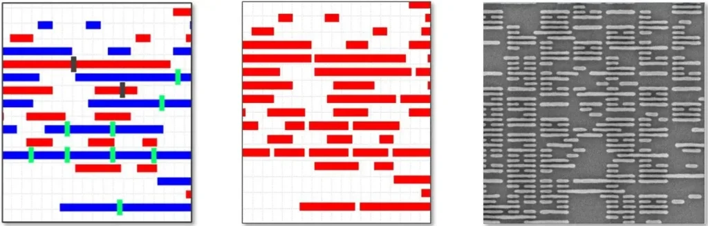
At the 2026 IEEE International Symposium on Circuits and Systems (ISCAS) in Shanghai, Huawei semiconductor president He Tingbo (pictured) delivered a speech titled “New Semiconductor Path in Practice” and said the company has developed a process called ‘Logic Folding’ by which it reduces the length of internal circuitry thereby cutting latency and improving performance.
Logic Folding technology operates under the ‘Tau Scaling Law’ which starts from the principle that scaling needs to focus as much on the circuitry as on on the transistors
“We believe that openness and collaboration are key to driving ongoing progress in the semiconductor industry,” said He, “no single company can independently find all the answers along the path of semiconductor evolution. With the τ Scaling Law, we look forward to working closely with scientists, engineers, and industry partners around the world to drive the sustainable development of the semiconductor and electronics industries.”
The Tau Law proposes replacing geometric scaling with time (τ) scaling as a new guiding principle for the evolution of both semiconductors and electronic systems.
Based on this principle, innovative technologies such as LogicFolding can be used to continuously compress signal propagation delay and steadily improve transistor density, which will drive the ongoing evolution of semiconductors and electronic systems.
Huawei said it had designed and mass-produced 381 chips over the past six years based on the Tau Scaling Law for applications including smartphones and computing.
Based on the Tau Law, LogicFolding can be used to continuously compress propagation delay which will, with improving transistor density, drive the ongoing evolution of semiconductors and electronic systems.
Huawei has established a multi-level co-optimization mechanism that spans semiconductor devices, circuits, chips, and systems. This mechanism aims to systematically shorten the time constant τ in order to drive up performance, energy efficiency, and transistor density at each level in the following ways:
At the device level: Optimizing the resistance and parasitic capacitance of transistors and interconnects to minimize the device-level time constant τ at the underlying physical layer
At the circuit level: Adopting the LogicFolding architecture to break down the physical boundaries of traditional circuit layouts, significantly shortening critical-path wiring, effectively reducing the resistive and capacitive load of signal propagation, and ultimately boosting transistor density and circuit performance
At the chip level: Employing full-stack coordinated design of software, architecture, and silicon to achieve fine-grained, workload-driven control over instruction and data flows, enhancing system-level parallelism and efficiency, and significantly reducing end-to-end execution time
At the system level: Redefining interconnect protocols for computing systems with UnifiedBus to achieve unified memory addressing and native memory semantics for SuperPoDs, significantly reducing system communications latency
The Kirin chips scheduled to launch in Fall 2026 will be the first to adopt the LogicFolding architecture, which will considerably enhance the chips’ performance.
By 2031, the high-end chips HUAWEI designs based on the τ Scaling Law are expected to feature a transistor density that is equivalent to 14 Å (1.4 nm) processes.