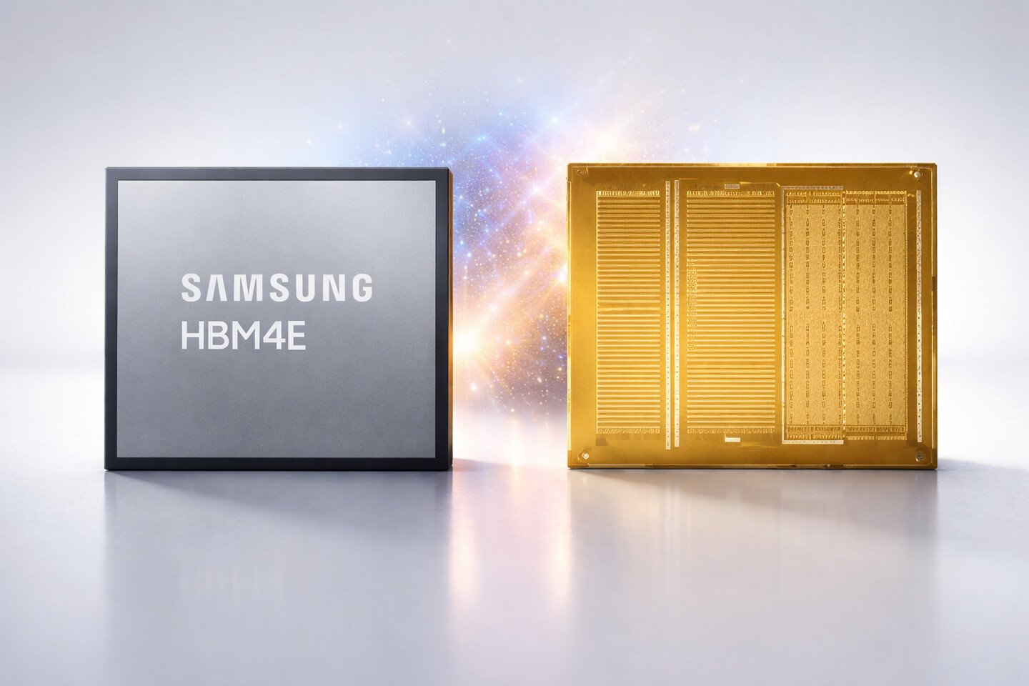
Samsung is reportedly planning to bring its 2 nm process to the base die of HBM4E, its 7th-generation high-bandwidth memory. This comes just a month after the company shipped the industry’s first commercial HBM4, and alongside a separate effort to redesign the HBM4E power delivery network to handle the increase in power bumps from 13,682 to 14,457 within the same footprint. Until HBM3, the base die had a somewhat passive role, sitting at the bottom of an HBM stack and handling power and signal control. Starting with HBM4, it took on a more active role by handling some compute tasks directly, making the underlying process node increasingly important. For HBM4, Samsung already had an edge here, using 4 nm logic base dies from its own foundry paired with its latest 1c DRAM, well ahead of the 12 nm (N12) process SK hynix sources from TSMC. Moving to 2 nm for HBM4E would extend that lead further, improving power efficiency, thermal management, and area utilization.
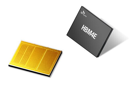
The other key players in the industry are also focusing on custom HBM4E as the next battleground, with TSMC stating it plans to use its 3 nm process for custom HBM4E, and SK hynix also working on its own variant. With its latest 2 nm node push, Samsung appears to be making a deliberate move to stay a step ahead on process technology. Standard HBM4E is expected mid-year, with custom product tape-in following in the second half of the year. The Business Korea report also points to the foundry angle. Producing HBM base dies internally helps Samsung Foundry keep fab utilization high, and the 2 nm node is expected to play a major role in ramping production at the Taylor fab in Texas. There, equipment installation is already underway, with the first wafer tape-in targeted before year-end.