Blog
The Evolution of Heterogeneous Integration and STCO

Advanced Connectivity and Hierarchical Planning
Driven largely by the demands of AI computing, modern chip designs often feature more than 50 million total pins and hundreds of thousands of connections, rendering traditional approaches to connectivity management obsolete.
To manage this explosion of die-to-die connections, designers are increasingly adopting language-based design. Writing Verilog RTL with proper bus notation is significantly more efficient and less error-prone than bit-by-bit spreadsheet definitions, which cannot scale to the millions of bumps required by hybrid and direct bonding technologies.
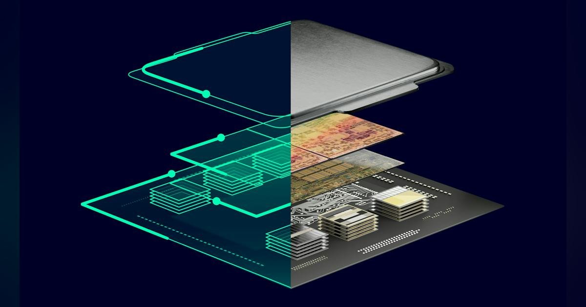
Hierarchical design further simplifies this complexity by disaggregating the system into manageable building blocks. By representing devices as hierarchical entities, designers can define topological pin regions using formulas, regular expressions, and design attribute tokens. Intelligent parametric pin regions enable the rapid creation and optimization of complex package designs. This allows for the efficient instantiation of silicon bridges and interposers, which act as low-latency, power-efficient wiring layers between CPUs, GPUs, and high-bandwidth memory (HBM) stacks.
Pathfinding and Predictive Multiphysics Analysis
A critical aspect of STCO is the ability to perform pathfinding, which means exploring different integration scenarios that align with the PPAC targets for the design.
To do this, engineers need to be able to view and manipulate all the building blocks of the system, including mechanical objects like heat spreaders and stiffeners, within a single cockpit. This allows for early assessment of how mechanical parts impact real estate and electrical clearances.
Predictive analysis is what makes or breaks this pathfinding process. For example, planning a power delivery network requires “shift-left” analysis to identify DC-drop issues early, prioritizing problem detection over absolute sign-off accuracy to prevent costly late-stage changes.
Similarly, early thermal evaluation is imperative in 3D ICs. Vertical chiplet stacking restricts traditional heat-removal paths through the top and bottom of the die. At the same time, thinning the dies increases lateral thermal resistance, making it more difficult for heat to escape through the sides of the chip. By using 3D-optimized EDA tools, engineers can model thermal gradients and mechanical stress across the entire assembly, ensuring that co-design optimizations do not introduce unmanageable reliability challenges.