Blog
Can Embedded Passives Fix AI’s Power Delivery Problem?

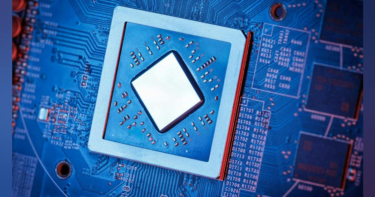
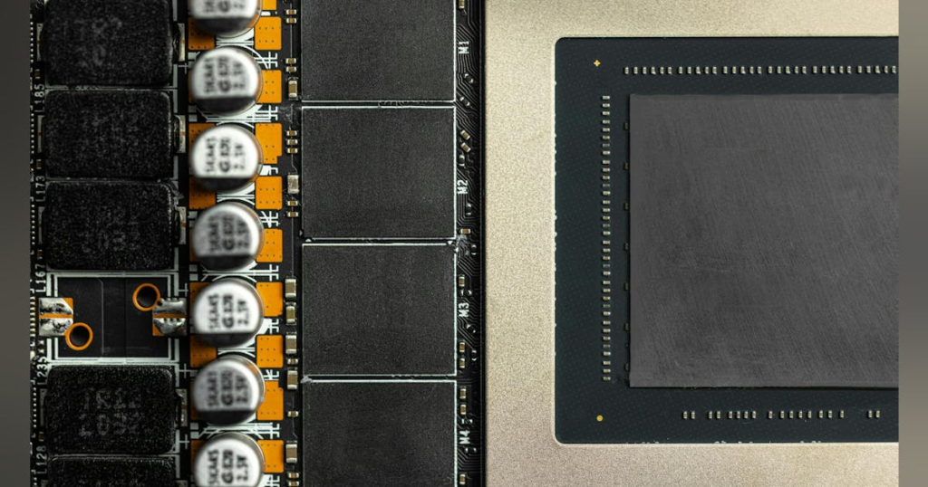
Most of the big names in power electronics are chasing the same challenge: Developing voltage regulators that can handle the huge currents required by GPUs and other kilowatt-class AI chips. But with lots of power comes lots of passive components. These DC-DC converters depend on increasingly large clusters of inductors and capacitors that convert, filter, and decouple the power delivered to the processor, helping maintain stable voltage and keeping current within the processor’s ripple envelope.
However, these passive components can hamper power delivery as much as they help it. They often occupy the most power-sensitive real estate on the PCB, forcing the DC-DC converter further from the load.
The added distance not only leads to higher power losses but also slows the system’s response to the large transient loads common with AI workloads. Moreover, the capacitors mounted under the board can crowd out vertical power delivery (VPD) solutions that could help tackle both issues.
One solution proposed by Saras Micro Devices is to combine the capacitors and inductors into a single module and integrate it into the processor’s package substrate. By bringing the regulators, passives, and compute die closer, Saras said it can reduce impedance in the power delivery network (PDN), improve efficiency, and enable tighter voltage regulation.
To learn more about its STILE technology and where it fits into the AI power picture, we reached out to Shaun Bowers, the startup’s SVP of Product Management.
When engineers talk about power delivery being a “bottleneck” for AI accelerators and other chips in the same high-performance ballpark, what do they mean?
The power “bottlenecks” that engineers talk about exist at multiple levels. At the highest level, the most fundamental issue is the imbalance between the rapidly rising demand for power to support and fuel the buildout of AI data centers and the less rapid buildout of grid infrastructure supporting this demand. This imbalance makes it imperative that every watt of power that is available and delivered to the AI data center is used in the most efficient way possible.
The next level at which a power delivery bottleneck exists is within the power delivery network (PDN) itself, all the way from the grid to the chip. However, this issue is particularly amplified as you get closer to the device.
With thermal design power (TDP) increasing to multi-kilowatt levels and data center power approaching gigawatt levels, the resistive losses in the PDN and heat generated by these losses are becoming too significant to ignore, particularly in an environment where the infrastructure needed to deliver the required power is already constrained.
To sustain growth and establish an economically viable business, it’s now critical to maximize the amount of compute per watt and minimize the cost per operation and token. Accomplishing this requires rethinking the PDN architecture at every step to maximize efficiency and minimize the associated heat load and power required for cooling.
Power delivery losses can add up from the rack to the chip. Where are those losses typically happening?
The losses from the rack to the chip occur during the various power-conversion steps within the PDN and from the resistive losses (I2R) associated with the distribution of that power to the chip. Today, most data center racks use a 54-V/48-V backplane as the primary power distribution system for the server, including the accelerator and processors.
On each accelerator and processor board, a 48- to 12-V voltage regulator module (VRM) is typically found along with a multitude of 12-V to point-of-load (POL) VRMs mounted on the board in a lateral arrangement around the chip that steps down from the 12-V input to the level required to service each of the power rails on the device.
As the level of silicon integration within the device goes up, the power density also increases to multiple kilowatts. At the same time, the advanced process nodes being used to fabricate the chips require lower operating voltages (0.6 to 0.8 V).
The net effect is that the amount of current that needs to be delivered by the PDN, from the VRM to the chip (I = P/V), is rising dramatically, and resistive losses in the PDN are growing exponentially with them.
Today’s systems rely on passive components in different locations to keep power stable, from the decoupling capacitors beneath the chip to bulk capacitors near the VRMs. Why do you need this hierarchy, and what are the limitations of the current approach?
The capability to correct voltage immediately during load changes is key to improving the system’s overall performance. Traditionally, parallel capacitors are used along the power delivery path as sources of charge to mitigate current surges quickly and stabilize voltage levels across the full frequency range of interest.
Each capacitor type is characterized by its impedance and the frequency range for which it is most effective. So, a capacitor network made up of multiple capacitor types, rather than just one type, is more effective in reducing impedance.
Today, the system must deliver an increasing amount of current. As the currents increase, more capacitance is needed, resulting in the need for more “critical” board-level real estate for power conversion and power delivery. Even as converter switching frequencies rise and converter sizes are reduced, passives remain a limiting factor.
How does Saras’ STILE technology fit into the power delivery network? Where is it located?
The STILE technology is an integrated passive “module” that is purposely designed for embedding into IC package substrates and system PCBs (Fig. 1). Unlike traditional ceramic passive components used in surface-mount applications, Saras’ capacitors are manufactured to match the thickness of the substrate where they’re going to be embedded. They’re fabricated with 3D pass-through copper terminations, exhibit almost no capacitance derating under temperature and bias, and are rated for operation at 125°C.