Blog
The quest for better chip design accelerates

Synopsys tackles some of the toughest problems in tech involving silicon design and simulation as the world seeks ways to economize when creating advanced AI chips and even various sensors and actuators fused to logic chips to tap into AI’s vast potential.
The biggest companies use Synopsys products in making chips like GPUs. They include Nvidia, Samsung, Mediatek and Cisco. Synopsys, in turn, uses some of the products those companies make. It faces competition from some giants: Cadence and Siemens, among others.
Nearly a year ago, Synopsys, based in Sunnyvale, Calif., closed on the purchase of Ansys for a staggering $35 billion, gaining access to what’s known as multiphysics simulation to add to Synopsys’ expertise with EDA tools and IP.
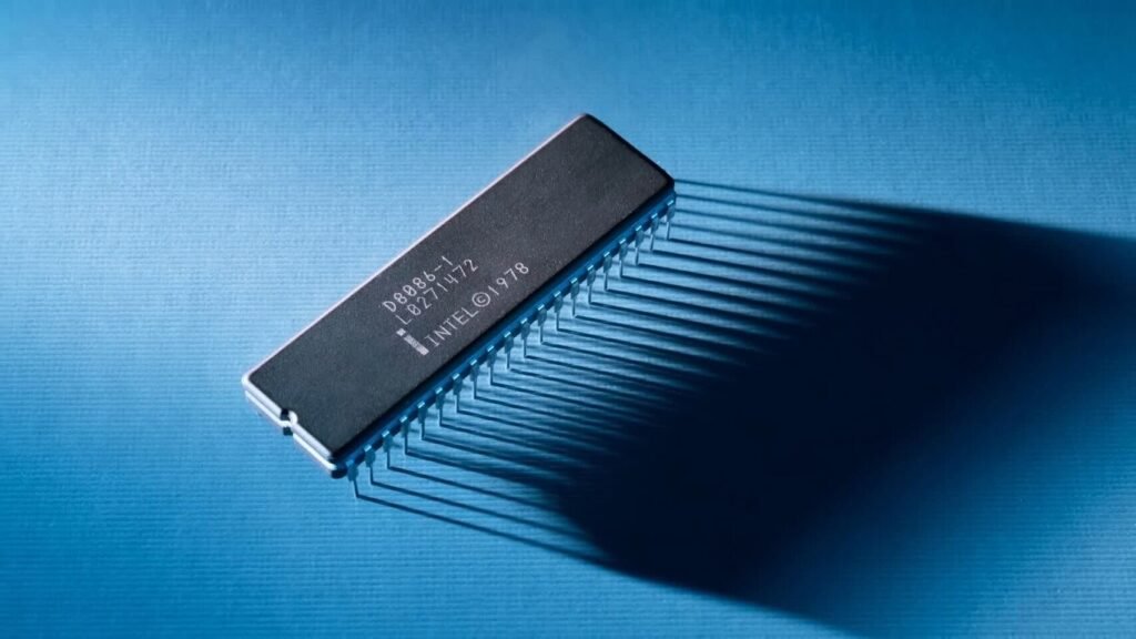
Electronic Design Automation is at the heart of everything happening in tech, allowing teams of chip design engineers to build chips with many billions of transistors inside, using the tools to design how each transistor behaves and to trace how much of a tiny amount of energy is needed to open or close a logic gate. They work in a field that insiders call “rocket science at a micro level.” Some of these design jobs are now being performed by AI agents, a field exploding in impact.
The purchase of Ansys theoretically turned Synopsys into a silicon-to-systems platform company, integrating electronics design with real-world physics in a single workflow. Synopsys sees itself as modeling the whole product–whether it is an EV or a robot or a satellite or even an AI chip for use in a data center–and not just the chip. This approach means multiphysics concerns around heat, power surges and drops, electromagnetic and mechanical effects (and more factors) are taken account earlier in the design cycle to save on the costs of a revision, often called a “respin.”
Synopsys announced its first wave of integration of Ansys tech into its product lineup in March, calling it Multiphysics Fusion. On Wednesday, it announced the general availability of Multiphysics Fusion to customers while naming Nvidia, Samsung Foundry, MediaTek and Cisco among early customers. In selected pilot designs, Nvidia reported it had seen 5x faster ability to finish designs, while Cisco said it gained earlier and more accurate visibility into real-world conditions with Multiphysics Fusion and a 20x faster runtime in its evaluations.
One area where Synopsys claims Multiphysics Fusion will help chip designers lower costs is by reducing “overdesign,” an industry term referring to designers’ tendency to add more silicon area to a chip to leave greater margin for unexpected results from heating and other physical effects.
Hany Elhak, executive director of product management and solutions at Synopsys, told Fierce that overdesign can stem from estimates of “IR drop” where the voltage supplied to components decreases as it travels through the chip’s power delivery network because of electrical resistance of metal wires. (IR means I for current and R is resistance). A drop in voltage can cause chip malfunctions and timing delays.
With greater insights Multiphysics Fusion supplies, Synopsys argues it can reduce overdesign of an advanced chip, which can lead to up to 35% wasted silicon area. That waste leads to a $250 million optimization loss on each advanced 2nm chip node in development, Synopsys said, basing its findings on TestFlow data.
“Co-design across domains enables early and more accurate design decisions” to help chip designers reduce overhead, Elhak said. Multiphysics Fusion will impact designs for chips used to fuse AI logic with sensors seen in robots and other physical AI. The latest announcement focuses on GPU-acceleration across four areas of Multiphysics Fusion: Timing Signoff, Design Closure, Multi-die Designs and Analog and Photonic Design.
Synopsys would not disclose the cost of Multiphysics Fusion products, pointing instead to the cost savings that Multiphysics Fusion would bring to a chip design firm.
Industry perspectives and analyst views
While Multiphysics Fusion is new on the market, it will likely challenge conventional EDA rivals like Cadence Design Systems which has capabilities in Computational Fluid Dynamics with the purchases of Pointwise and NUMECA in 2021. Another major EDA rival is Siemens, active in the electrical-mechanical co-design space.
At Computex Taipei in early June, Cadence and Nvidia jointly announced an autonomous virtual agentic AI design engineer which uses Cadence EDA with Nvidia’s Nemotron models to enable customers to run dynamic simulations in automated workflows for use in designing Level 5 autonomy for vehicles. The ChipStack AI Super Agent runs within the Nvidia OpenShell runtime and shrinks validation cycles from weeks to less than a day, the companies claimed. The level 5 capabilities in ChipStack will be available in the second half of 2026.
Fierce asked principal analyst Dave Altavilla at HotTech Vision and Analysis how Synopsys’ Multiphysics Fusion is different from what’s been on the market. He responded that chip designers have always accounted for physical effects such as thermal behavior, power delivery and signal integrity. What’s changed, he said, “is the scale and complexity” of making new chips that are 2.5D or 3D and use disparate materials, some with chiplets using different processors.
Altavilla elaborated: “With modern chip design in advanced process nodes, especially with chiplets, stacked memory, advanced packaging and co-packaged optics, these physical interactions can no longer be treated as isolated verification steps performed late in the design cycle. A thermal hotspot in one die can affect timing in another. Package design decisions can influence power integrity. Mechanical stress can alter transistor behavior…
“The significance of Synopsys’ Multiphysics Fusion approach is about reducing the friction between design and analysis workflows, allowing engineering teams to make better-informed decisions before problems become expensive to fix…The opportunity here with Synopsys Multiphysics Fusion is to bring more of that analysis earlier into the design process where engineering teams still have flexibility to make changes that cost far less and reach desired outcomes earlier. With silicon on the cutting edge, avoiding a delay or a respin can easily justify the investment with the opportunity to reap cost and time-to-market savings exponentially…”
The need for these insights is “very real…the need to co-optimize chip, package and system design is more critical than ever,” he added.