Blog
New substrate for ceramic packages allows high density wiring and delivers greater rigidity
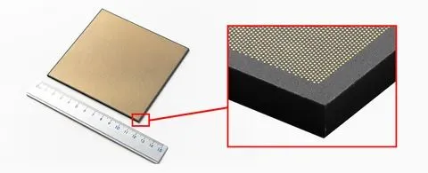
Built from Kyocera’s proprietary Fine Ceramic materials, the substrate is engineered for high‑density wiring and exceptional rigidity.
According to the company, these characteristics dramatically reduce deformation (warpage) in high-performance semiconductor packages, a key challenge as demand for greater device integration and higher processing speed continues to rise.
Features
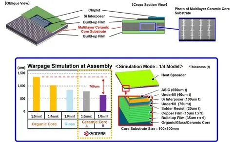
1. Highly rigid multilayer ceramic core substrate minimizes warpage, a key challenge affecting large package substrates
Kyocera’s multilayer ceramic core substrate provides greater rigidity and resistance to deformation (bending) than core substrates made of organic materials, minimizing warpage during each mounting phase. As a result, Kyocera’s multilayer ceramic technology can enable higher device performance using slimmer substrates while facilitating further miniaturization.
2. Multilayer ceramic structure enables finer wiring
In multilayer ceramic substrates, conductive paths between layers of ceramic are called vias. Formed while the ceramic is pliable (before firing or sintering), these vias enable finer wiring through superior micro-fabrication as compared to the drilling processes used to create vias in conventional organic core substrates. The smaller via diameters and tighter via pitches made possible in ceramic substrates address the challenges associated with high-density wiring in traditional organic-core substrates.
3. Supports custom design requirements, and performance simulations in the design phase
During the design phase, Kyocera provides thermal, electrical, and substrate-warpage simulations based on device performance objectives and specified mounting processes. This simulation data ensures greater customer development efficiency and the achievement of design objectives in the finished device
See all our Kyocera content.