Blog
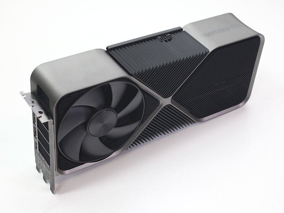
NVIDIA GeForce RTX 3060 12 GB Returns in June, RTX 5050 9 GB Edition on Pause
The NVIDIA GeForce RTX 3060 features 3,584 CUDA cores and 12 GB of GDDR6 memory. In contrast, the GeForce RTX 5050 has newer CUDA cores on a smaller node with 2,560 cores on the GB207 die, but it has less memory, with only 9 GB of the rumored GDDR7. Since the resurrected GeForce RTX 3060 will use the older GDDR6 memory, sourcing GDDR6 may have been easier for NVIDIA, leaving the more expensive GDDR7 for its other GPUs.
Additionally, the decision to use a two-generations-old GPU architecture in 2026 is puzzling, as the reason NVIDIA has chosen the RTX 3060 instead of a newer model like the RTX 4060 remains unclear. Speculatively, it could be because the RTX 4060 is based on the same NVIDIA 4N (5 nm-class) node at TSMC as the current RTX 5060, while the RTX 3060, along with the rest of the GeForce “Ampere” generation, is built on the Samsung 8N (8 nm DUV) foundry node. This would leave the 5 nm capacity for “Blackwell” and its enterprise variants. Finally, it’s worth noting that when GPU IP design is completed, it is usually hard-linked with the node it was prepared for, so NVIDIA is sticking with Samsung again to avoid any potential upfront costs of adapting this GPU for a different node.