Blog
IBM 7-Angstrom Technology Packs in 100 Billion Transistors

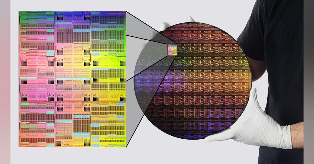
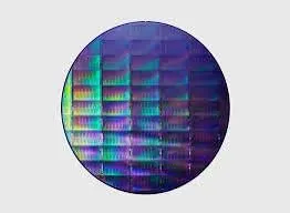
Smaller transistors usually mean better performance and greater power efficiency. In this case, the new 7-Å devices bump up performance by 50% while improving power utilization by 70% compared to IBM’s 2-nm node.
Designers still have the reticle limit when it comes to production, but making transistors smaller means packing in more within that limit. Packaging technologies like chiplets allow designers to build systems that would not be possible with a single die. Chiplets also make it possible to mix die with different transistor technologies and different functionality like high bandwidth memory (HBM).
3D die stacking has been common with solutions like HBM. However, this technology layers die atop each other. The nanostack does it at the transistor level albeit with only a few levels (Fig. 2). IBM’s research has projected that a 4-track staggered design will deliver a 50% area improvement while reducing power requirements. Both are designed to increase density.
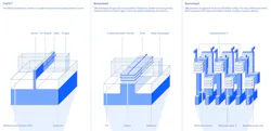
IBM’s nanostack configuration is built on a multichannel, nanosheet-on-nanosheet NanoStack CMOS architecture. It employs a vertical inter-FET isolation.
The company’s announcement is about the technology and possibilities rather than release of production devices, but that will come. In the meantime, these announcements highlight how the next generation of electronic devices will be constructed.