Blog
Samsung Exynos 2600 SoC Annotated, Showcases 3-tier CPU, AMD RDNA 4 iGPU

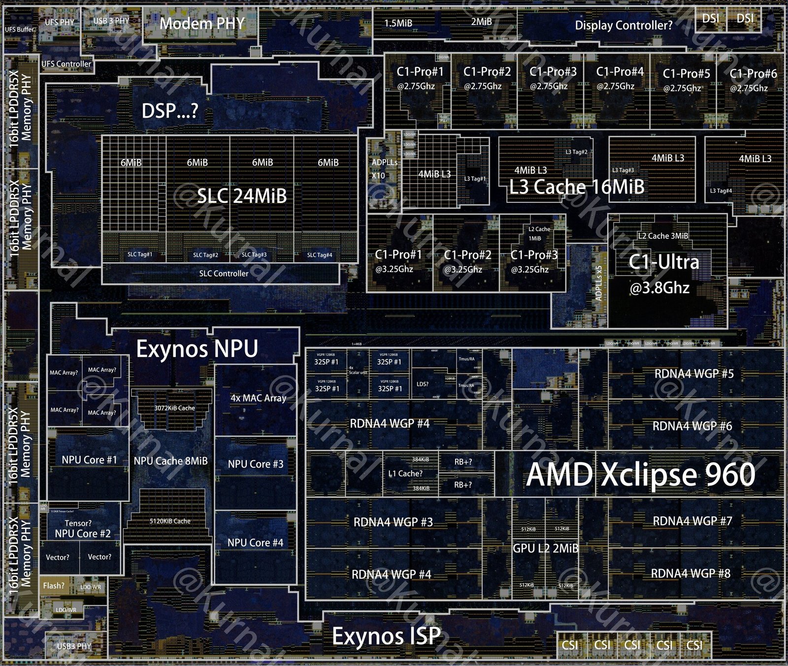
We begin our tour with the CPU. Samsung designed the Exynos 2600 with a 3-tiered heterogenous multicore design, and a 1X+3P+6E core configuration. Leading it is one C1-Ultra extreme core that ticks at up to 3.80 GHz, offers the highest IPC, and comes with 3 MB of dedicated L2 cache. Next to it are three C1-Pro performance cores, which run at up to 3.25 GHz, and handle most performance-heavy workloads. Each C1-Pro core has 1 MB of dedicated L2 cache. Trailing these are six other C1-Pro cores, which are purposed to serve as efficiency cores. Their clock speed only runs up to 2.75 GHz, and have a more aggressive power-management scheme. The “P-cores” and “E-cores” on this chip are functionally identical, and have the same transistor count, but are simply configured differently. The CPU complex is held together by 16 MB of shared L3 cache that all 10 cores have equal access to.
The next major component is the Xclipse 960 iGPU, which has been licensed as an IP block to Samsung by AMD. The Xclipse 960 is powered by AMD’s latest RDNA 4 graphics architecture, which inherits all the LPDDR memory-management optimizations from its predecessor, RDNA 3.5. The iGPU has 16 compute units spread across eight workgroup processors (WGPs), which total 1,024 stream processors, besides 64 TMUs and 32 ROPs. The GPU has 4 MB of dedicated L2 cache.
The third major component is the NPU, which Samsung designed to offer an over 100% increase in performance over the NPU of Exynos 2500. It features a 32K MAC design spread across cores, each with four MAC arrays, each with dedicated Tensor and vector hardware. The six cores are cushioned by an 8 MB scratchpad RAM. This NPU offers a real-world throughput of 59 TOPS.
Elsewhere across the chip, we see image processors, DSPs, display controllers, media accelerators, and an on-chip non-volatile storage medium with 24 MB of system-level cache. I/O interfaces include a 64-bit LPDDR5X memory interface, UFS PHY, multiple USB 3.2 PHYs, and eDP for display.