Blog
Metrology tools for wire bonded chips
View Micro Metrology is a New York-based metrology company which offers software and algorithms to meet the precision manufacturers need. It announced that it is focusing on 10-12µm diameter wire-bonded chips and 15-30mm via inspection.
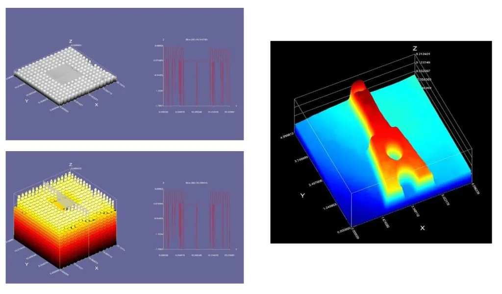
Its portfolio includes edge-detection algorithms and proprietary optical auto-focus technologies for advanced semiconductor packaging to provide insights into critical dimensions, including solder ball positions relative to pads and leads, ball heights, and loop heights. The company has been evaluating a variety of wire‑bonded packages, including both relatively straight wire profiles and high loop geometries. The issue with wire loop height inspection is that the highest point is often extremely small and on a reflective surface.
In addition to edge-detection algorithms for wire bond and interconnect applications, its software can acquire full frame, megapixel, digital images in real time using Area Multi-Focus (AMF) which creates a high-resolution 3D data set from a normal auto focus pass to serve as an alternative to single point laser surface scanning. An extended depth of field image can be simultaneously created for an in-focus image. Other technology is Continuous Image Capture (CiC) which synchronises illumination with camera frame acquisition and movement to acquire continuous video images. This can improve throughput by 50%-200% said the company, for components with densely packed features, compared to standard move-and-measure techniques.
There are also image filtering options to process the videos and a library of tools for image display and analysis for use in automated edge detection and area processing operations.
View spoke to Electronics Weekly at Microelectronics US in Austin, Texas. Read more news from the event:
Destination Austin – Microelectronics US focuses on industry supply chain